How to build object detection application on STM32N6570-DK
This tutorial will guide you through the essential steps to build an object detection demo application on the STM32N6570-DK evaluation board.
Introduction
The application's workflow consists of:
- Capturing images from the camera.
- Displaying the live feed on the LCD.
- Resizing and formatting the images for the object detection model.
- Running inference and processing the model’s output to generate accurate detection results.
Note: A basic understanding of embedded systems is recommended to easily follow along with this tutorial.
This tutorial focuses specifically on the code modifications and updates required after generating the base project with STM32CubeMX. The covered topics include:
- Adding the required middleware components and drivers
- Configuring the DCMIPP (Digital Camera Memory Interface Pixel Processor) pipelines
- Initializing and running the object detection model
- Managing LCD display
- Processing inference outputs
- Building & Flashing
The Git repository of this tutorial ( see related links) contains the project .ioc file,
the trained neural network model, the project dependencies, and the complete application source code.
A separate tutorial may be published later to explain the .ioc configuration process step by step.
Middleware & Drivers
Start by copying the necessary drivers and middleware from the STM32Cube firmware package to your project.
Copy Drivers
From:
C:\Users\UserName\STM32Cube\Repository\STM32Cube_FW_N6_V1.3.0\DriversCopy the following folders into your project:
BSP\Components→ProjectRoot\Drivers\BSPBSP\STM32N6570-DK→ProjectRoot\Drivers\BSPCMSIS\DSP→ProjectRoot\CMSIS
Copy Middleware
From:
C:\Users\UserName\STM32Cube\Repository\STM32Cube_FW_N6_V1.3.0\Middlewares\STCopy:
STM32_ISP_Library→ProjectRoot\Middlewares\ST
Adding Camera and Board Support Files
In: ProjectRoot\Appli\Driver\Components
Create a new folder: imx335
Add the following source files:
imx335.cImx335_reg.c
In: ProjectRoot\Appli\Driver\STM32N6570-DK
Add the following board support files:
stm32n6570_discovery.cStm32n6570_discovery_bus.c
In: ProjectRoot\Appli\Middlewares
Add ISP middleware integration files:
isp_algo.cisp_core.cIsp_services.c
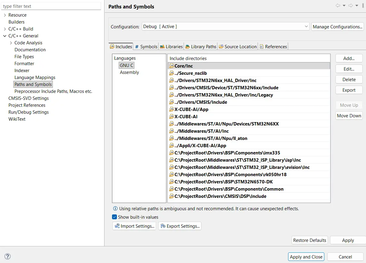
Configuring the Project in STM32CubeIDE
Navigate to:
Project_Appli → Properties → C/C++ General → Paths and SymbolsAdd all required include directories as shown in this figure.
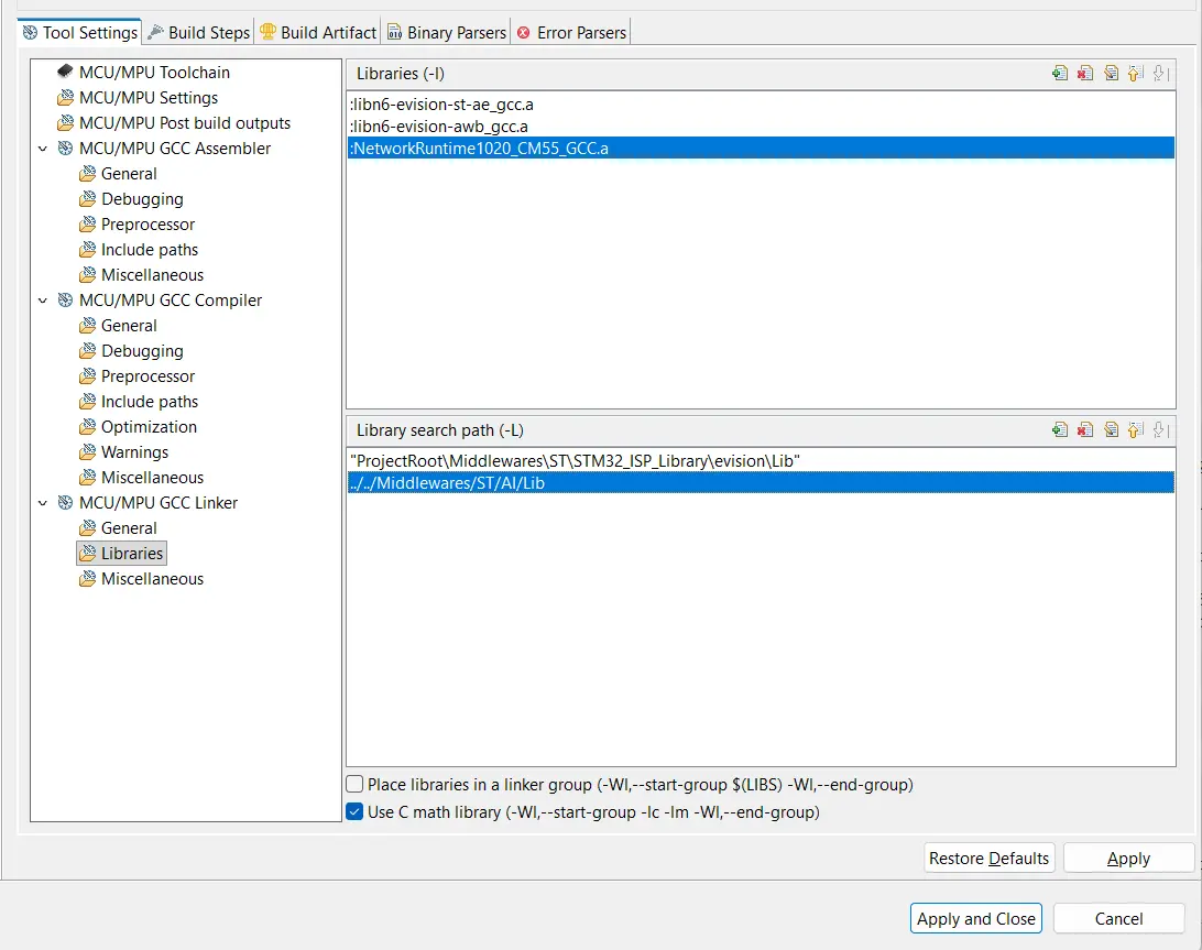
Navigate to:
Project_Appli → Properties → C/C++ Build → Settings → MCU/MPU GCC Linker → LibrariesAdd the required library paths and link the necessary Evision libraries as shown in this figure.
The last step is to add the header and source files from
Appli\Core in the Git repository to the core of your project.
DCMIPP Configuration
Correctly configuring the digital camera interface pixel pipeline (DCMIPP) is a key factor in building this demo. Let us first understand what the DCMIPP is and how it can be configured.
The camera module can interface with the MCU using either a parallel or Camera Serial Interface 2 (CSI-2) communication protocol. The CSI-2 Host controller connects external serial cameras through dedicated clock and data lanes, enabling the transmission of image data from CSI-2 compliant camera sensors to the DCMIPP for further processing.
In other words, the DCMIPP receives pixel data from either a parallel interface or a CSI-2 interface. Once the pixel stream enters the DCMIPP, a flow selector routes the data to the appropriate processing pipeline, where the processed pixels are written into predefined memory buffers.
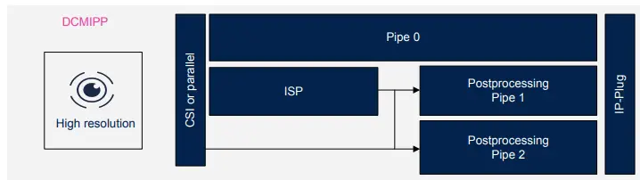
The DCMIPP architecture features three main pipelines: Pipe 0, Pipe 1, and Pipe 2. In this tutorial, Pipe 1 is used for image display, while Pipe 2 is dedicated to the object detection model. Therefore, the focus will be on configuring these two pipelines. Readers can refer to the official STM documentation for more details about Pipe 0.
The DCMIPP also integrates Image Signal Processing (ISP) functions within Pipe 1 (shared with Pipe 2) as shown in the following figure. In addition, each pipeline provides dedicated post-processing functions such as cropping, downsampling, resizing, and pixel format conversion.
These post-processing stages adapt the captured image to the requirements
of the target application. For example, the IMX335 image sensor camera
used in this tutorial captures images at a resolution of
2592 × 1944 pixels, while the YOLO model expects an input
resolution of only 192 × 192 pixels.
ISP Configuration
The Image Signal Processor (ISP) processes raw data coming from the camera sensor to produce a full-resolution RGB image. It performs key tasks such as white balance, color space conversion, Bayer pattern reconstruction, and bad pixel correction.
These functions are particularly important for camera modules that output raw Bayer data and do not include an internal ISP pipeline, which is the case in this tutorial using the IMX335 image sensor.
The ISP configuration used in this tutorial is based on the
DCMIPP_SnapshotDecimationMode example provided by
STMicroelectronics.
The initialization sequence for the ISP is as follows:
- Start acquisition on Pipe 1 and enable the ISP
- Configure color balance parameters
- Stop acquisition after initialization and configuration are completed
			/* Fill init struct with Camera driver helpers */
			ISP_AppliHelpersTypeDef appliHelpers = {0};
			appliHelpers.GetSensorInfo = GetSensorInfoHelper;
			appliHelpers.SetSensorGain = SetSensorGainHelper;
			appliHelpers.GetSensorGain = GetSensorGainHelper;
			appliHelpers.SetSensorExposure = SetSensorExposureHelper;
			appliHelpers.GetSensorExposure = GetSensorExposureHelper;

			/* Initialize the Image Signal Processing middleware */
			if(ISP_Init(&hcamera_isp, &hdcmipp, 0, &appliHelpers, ISP_IQParamCacheInit[0]) != ISP_OK)
			{
				Error_Handler();
			}

			if (HAL_DCMIPP_CSI_PIPE_Start(&hdcmipp, DCMIPP_PIPE1, DCMIPP_VIRTUAL_CHANNEL0, BUFFER_ADDRESS, DCMIPP_MODE_CONTINUOUS) != HAL_OK)
			{
				Error_Handler();
			}

			/* Start the Image Signal Processing */
			if (ISP_Start(&hcamera_isp) != ISP_OK)
			{
				Error_Handler();
			}

			/* give the ISP 60 frames to set color balance */
			while(NbMainFrames < 60)
			{
				while(pipe1_frame_ready == 0)
				{
				}

				pipe1_frame_ready = 0;
				NbMainFrames++;

				BSP_LED_Toggle(LED_GREEN);

				if (ISP_BackgroundProcess(&hcamera_isp) != ISP_OK)
				{
					BSP_LED_Toggle(LED_RED);
				}
			}

			NbMainFrames = 0;

			/* stop the acquisition */
			HAL_DCMIPP_CSI_PIPE_Stop(&hdcmipp, DCMIPP_PIPE1, DCMIPP_VIRTUAL_CHANNEL0);
To get information when the frame of Pipe 1 or Pipe 2 is ready, we overloaded HAL_DCMIPP_PIPE_FrameEventCallback function in main.c.
				void HAL_DCMIPP_PIPE_FrameEventCallback(DCMIPP_HandleTypeDef *hdcmipp, uint32_t Pipe)
				{

				  if (Pipe == DCMIPP_PIPE2)
				  {
					pipe2_frame_ready = 1;
				  }
				  if (Pipe == DCMIPP_PIPE1)  {
					pipe1_frame_ready = 1;
				  }
				}
Pipe 1 & Pipe 2 Configurations
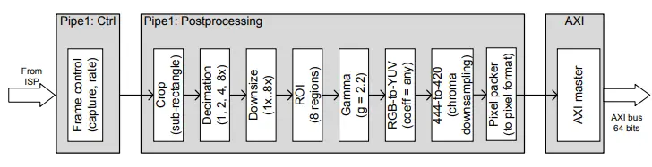
The figure below shows the pixel pipeline of Pipe 1 and Pipe 2, where post-processing functions are integrated.
When the LCD is enabled (the USE_LCD parameter in
main.h is set), Pipe 1 is used for image display,
while Pipe 2 is used for the NN model.
When the LCD is disabled, Pipe 1 is used for NN processing.
Before configuring the post-processing functions for each pipeline, some configurations are shared between both pipes. These include parameters such as:
DataLaneMappingPHYBitrateDataTypeModeDataTypeIDA
These settings are configured after creating an instance of the
DCMIPP_HandleTypeDef structure by initializing its members.
The corresponding code is part of the
MX_DCMIPP_Init function in main.c.
			DCMIPP_CSI_PIPE_ConfTypeDef pCSIPipeConf = {0};
			DCMIPP_CSI_ConfTypeDef csiconf = {0};

			hdcmipp.Instance = DCMIPP;

			if (HAL_DCMIPP_Init(&hdcmipp) != HAL_OK)
			{
				Error_Handler();
			}

			/* Configure the CSI */
			csiconf.DataLaneMapping = DCMIPP_CSI_PHYSICAL_DATA_LANES;
			csiconf.NumberOfLanes   = DCMIPP_CSI_TWO_DATA_LANES;
			csiconf.PHYBitrate      = DCMIPP_CSI_PHY_BT_1600;

			if(HAL_DCMIPP_CSI_SetConfig(&hdcmipp, &csiconf) != HAL_OK)
			{
				Error_Handler();
			}

			/* Set Virtual Channel config : Channel 0 */
			if(HAL_DCMIPP_CSI_SetVCConfig(&hdcmipp, DCMIPP_VIRTUAL_CHANNEL0, DCMIPP_CSI_DT_BPP10) != HAL_OK)
			{
				Error_Handler();
			}

			/* Configure the serial Pipe */
			pCSIPipeConf.DataTypeMode = DCMIPP_DTMODE_DTIDA;
			pCSIPipeConf.DataTypeIDA  = DCMIPP_DT_RAW10;
			pCSIPipeConf.DataTypeIDB  = DCMIPP_DT_RAW10;

			uint32_t NN_pipe = DCMIPP_PIPE2;

			if(USE_LCD == 0)
			{
				NN_pipe = DCMIPP_PIPE1;
			}

			for (uint32_t i = DCMIPP_PIPE1; i ≤ NN_pipe; i++)
			{
				if (HAL_DCMIPP_CSI_PIPE_SetConfig(&hdcmipp, i, &pCSIPipeConf) != HAL_OK)
				{
					Error_Handler();
				}
			}
Pipe 2 Configuration
The output dimension of Pipe 2 depends on the input model dimension.
In order to convert an image from
1944 × 2592 (camera output)
to 192 × 192 (model input),
cropping, decimation, and downsampling are used.
Cropping: The output of this step is a square image of size 1944 × 1944.
					DCMIPP_CropConfTypeDef crop_conf = {0};

					crop_conf.Vstart = 0;
					crop_conf.Hstart = 324;
					crop_conf.VSize = 1944;
					crop_conf.HSize = 1944;

					HAL_DCMIPP_PIPE_SetCropConfig(hcamera_dcmipp, pipe2, &crop_conf);

					HAL_DCMIPP_PIPE_EnableCrop(hcamera_dcmipp, pipe2);
Decimation: Converts the 1944 × 1944 image into 972 × 972.
			DCMIPP_DecimationConfTypeDef dec_conf = {0};

			dec_conf.VRatio = DCMIPP_VDEC_1_OUT_2;
			dec_conf.HRatio = DCMIPP_HDEC_1_OUT_2;

			HAL_DCMIPP_PIPE_SetDecimationConfig(hcamera_dcmipp, pipe2, &dec_conf);

			HAL_DCMIPP_PIPE_EnableDecimation(hcamera_dcmipp, pipe2);
Note: The enumeration values must be taken from
stm32n6xx_hal_dcmipp.h when configuring decimation.
192 × 192).
			DCMIPP_DownsizeTypeDef down_conf = {0};

			ratio_width  = 972 / 192;
			ratio_height = 972 / 192;

			down_conf.HRatio = (uint32_t)(8192 * ratio_width);
			down_conf.VRatio = (uint32_t)(8192 * ratio_height);

			down_conf.HDivFactor = (1024 * 8192 - 1) / down_conf.HRatio;
			down_conf.VDivFactor = (1024 * 8192 - 1) / down_conf.VRatio;

			down_conf.HSize = 192;
			down_conf.VSize = 192;

			HAL_DCMIPP_PIPE_SetDownsizeConfig(hcamera_dcmipp, pipe2, &down_conf);

			HAL_DCMIPP_PIPE_EnableDownsize(hcamera_dcmipp, pipe2);
Pipe 1 Configuration
In this tutorial, the configuration of Pipe 1 depends on the displayed
frame size. This size is defined by the
ASPECT_RATIO_MODE parameter in main.h.
- The displayed frame is cropped identically to the NN input.
- The Pipe 1 configuration is identical to Pipe 2.
-
The displayed frame is resized to fit into a square with a side
equal to the LCD display height (
480 × 480). - Cropping and decimation stages are skipped.
- Downsampling is configured using the following ratios.
			ratio_width  = 2592 / 480;
			ratio_height = 1944 / 480;

			down_conf.HSize = 480;
			down_conf.VSize = 480;
- The frame is displayed full screen.
- Cropping and decimation stages are skipped.
- Downsampling is configured using the following ratios.
			ratio_width  = 2592 / 800;
			ratio_height = 1944 / 480;

			down_conf.HSize = 800;
			down_conf.VSize = 480;
Notes
- Gamma conversion is already handled by the ISP (Image Signal Processor) functions.
-
The buffer address of Pipe 1, when the LCD is enabled,
is
0x34200000. - This is the memory address from which the LCD reads data for display.
-
Pixel packer configuration:
-
For Pipe 2:
DCMIPP_PIXEL_PACKER_FORMAT_RGB888_YUV444_1 -
For Pipe 1:
DCMIPP_PIXEL_PACKER_FORMAT_RGB565_1
-
For Pipe 2:
-
The user can configure the following parameters in
main.h:- Input model dimensions
- Camera resolution
- USE_LCD
-
Pipe 1 and Pipe 2 are configured in
NN_processing.h. -
The values of the crop, decimation, and downsize structures are
computed automatically in
cameraPipelineUtils.c. -
USE_LCD = 0→ Pipe 2 is deactivated, and Pipe 1 is used for the NN model.
Object Detection Model
The functions developed in this example to initialize the NN model
and run inference are inspired by the template functions generated
by STM32CubeMX in app_x-cube-ai.c.
The NeuralNetwork_init function initializes the model
and gets the input and output buffer information.
The input buffer is mapped directly to the DCMIPP pipe dedicated to
the NN model, which automatically stores a newly captured and resized
image after each frame.
Meanwhile, the output buffer holds the raw predictions, which are then processed to extract relevant object detection information.
void NeuralNetwork_init(uint8_t **nn_in, uint8_t **nn_out, uint32_t *nn_in_length, uint32_t *nn_out_len)
			{
			   const LL_Buffer_InfoTypeDef *ibuffersInfos = NN_Interface_Default.input_buffers_info();

			   const LL_Buffer_InfoTypeDef *obuffersInfos = NN_Interface_Default.output_buffers_info();

			   /* Get input/output buffer addresses */
			   *nn_in  = (uint8_t *)LL_Buffer_addr_start(&ibuffersInfos[0]);
			   *nn_out = (uint8_t *)LL_Buffer_addr_start(&obuffersInfos[0]);

			   /* initialize runtime */
			   LL_ATON_RT_RuntimeInit();

			   /* init model instance */
			   LL_ATON_RT_Init_Network(&NN_Instance_Default);

			   /* Get input buffer size */
			   *nn_in_length = ibuffersInfos->offset_end - ibuffersInfos->offset_start;

			   /* Get output buffer size */
			   *nn_out_len = (obuffersInfos->offset_end - obuffersInfos->offset_start);
			}
Running Inference
To run the inference, the dedicated inference function is called. Each time it executes, it processes the image data currently stored in the input buffer and writes the resulting predictions into the output buffer.
			void Run_Inference()
			{
				LL_ATON_RT_RetValues_t ll_aton_rt_ret = LL_ATON_RT_DONE;

				do {
					/* Execute first/next step */
					ll_aton_rt_ret = LL_ATON_RT_RunEpochBlock(&NN_Instance_Default);

					/* Wait for next event */
					if (ll_aton_rt_ret == LL_ATON_RT_WFE) {
						LL_ATON_OSAL_WFE();
					}

				} while (ll_aton_rt_ret != LL_ATON_RT_DONE);

			}
Processing the Output
Processing the output depends on the specific characteristics of your network. In this tutorial, a YOLO model is used, where the 1D output buffer is divided into segments.
Each segment represents the output of a single grid cell, and the length of each segment is equal to:
Number of Anchors × (5 + Number of Classes)
float *output = (float *)nn_out;

SCB_InvalidateDCache_by_Addr((uint32_t*)nn_out, nn_out_len);

postProcessing_NN_output(output, nn_out_len/4, detections, &out_count, max_detection, threshold);
A deep dive into the internal architecture of YOLO is outside the scope of this tutorial. In this specific example, the model output consists of floating-point values. However, in many edge AI applications, the model output is quantized (integer-based).
To dequantize the output back into a standard float, apply the following formula:
Float = (output - offset) × scale
The specific offset and scale values for the output layer are stored
in the scale and offset attributes of the
output model structure. These values can be retrieved in the NeuralNetwork_init function using:
const LL_Buffer_InfoTypeDef *obuffersInfos = NN_Interface_Default.output_buffers_info();
LCD
The LCD is connected to the frame buffer located at address
0x03420000. This address is mapped to Pipe 1 of the DCMIPP, which is dedicated
to image display on the LCD.
To use the LCD, the following steps are required:
-
Initialize the LCD
- Initialize the LCD using the screen width and height parameters.
-
LCD_Init(SCREEN_WIDTH, SCREEN_HEIGHT); -
The
LCD_Initfunction is derived from theDCMIPP_SnapshotDecimationModeexample and is implemented inmain.cwithin the application project.
-
Configure Display Window
- Configure the display window size (if different from screen resolution).
-
This is required for
ASPECT_RATIO_FITandASPECT_RATIO_CROPmodes. -
HAL_LTDC_SetWindowSize(&hltdc, lcd_width, lcd_height, LTDC_LAYER_1);
Once the LCD is initialized and the window is set, it continuously
refreshes and displays the contents of the buffer located at
0x03420000.
Build & Flash
The STM32N6 microcontroller series is based on the Arm® Cortex®-M55 core, which enables secure boot by default. Consequently, every binary file must be signed before it can be flashed and executed.
However, manually signing binaries during active development quickly becomes repetitive and time-consuming—especially for applications like this example that require two image stages.
By integrating the signing tool directly into the STM32CubeIDE build pipeline, you can automate the signing process so trusted binary files are generated automatically after every build operation.
In this example, we will automate the signing of two binary files:
-
ProjectRoot/FSBL/Debug/<Your_Project_Name>_FSBL.bin -
ProjectRoot/Appli/Debug/<Your_Project_Name>_Appli.bin
The automated post-build process should generate:
<Your_Project_Name>_FSBL-trusted.bin<Your_Project_Name>_Appli-trusted.bin
Setup post-build automation
- Right-click on your project in the STM32CubeIDE Project Explorer
- Select Properties
- Navigate to C/C++ Build → Settings
- Select the Build Steps tab
- Paste the command into the Post-build steps text box
- Apply the changes and exit
cd "${ProjDirPath}/Debug" && echo y | "C:\Program Files\STMicroelectronics\STM32Cube\STM32CubeProgrammer\bin\STM32_SigningTool_CLI.exe" -bin "${ProjName}.bin" -nk -of 0x80000000 -t fsbl -o "${ProjName}-Trusted.bin" -hv 2.3 -dump "${ProjName}-Trusted.bin" -align
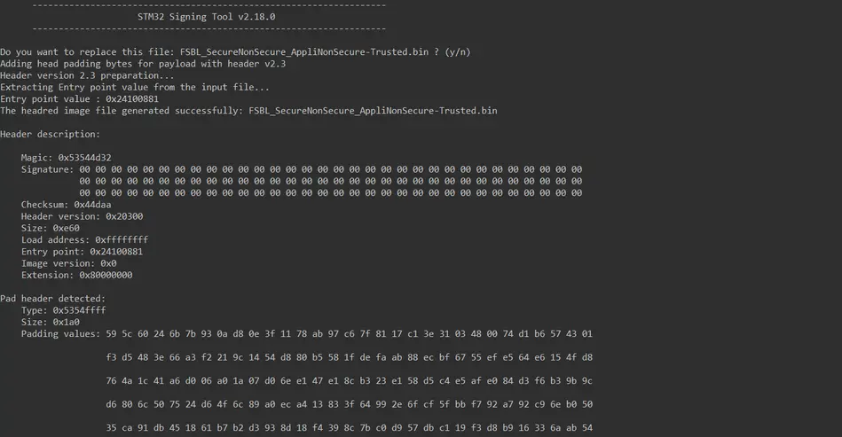
⚠️ Compatibility Note:
If you are using STM32CubeProgrammer version 2.20.0 or older, the
-align flag is not supported. Remove -align
from the command to avoid build errors.
For reference, the terminal output should look like:
Convert the model weights to Hex image
network_atonbuf.xSPI2.raw is generated by X-CUBE-AI in STM32CubeMX.
In this case, we rename and convert this file to: network_data.xSPI2.bin
cp network_atonbuf.xSPI2.raw network_data.xSPI2.bin
Next, convert the .bin file into a .hex file mapped
to a specific external flash memory address (0x71000000).
Open a command prompt or terminal and navigate to the GNU toolchain binary directory used by STM32CubeIDE. For example (STM32CubeIDE 1.18.1):
C:\ST\STM32CubeIDE_1.18.1\STM32CubeIDE\plugins\com.st.stm32cube.ide.mcu.externaltools.gnu-tools-for-stm32.12.3.rel1.win32_1.1.100.202509120712\tools\bin
Then run the following command:
arm-none-eabi-objcopy -I binary "C:\Path\To\ProjectRoot\network_data.xSPI2.bin" --change-addresses 0x71000000 -O ihex "C:\Path\To\ProjectRoot\network_data.hex"
Flash
- Set your board to dev mode (Boot1 and Boot2 to the L position)
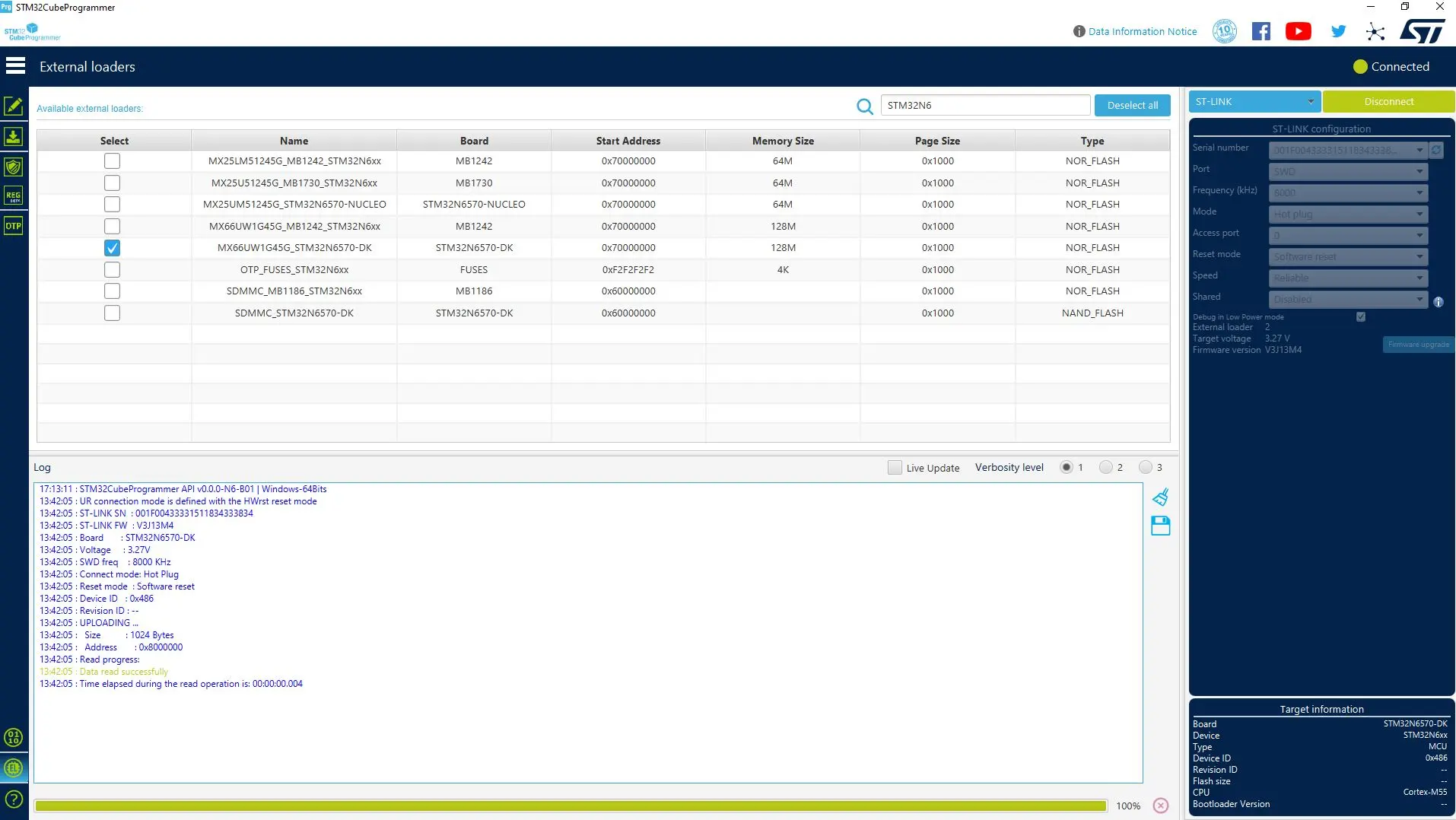
- Open STM32CubeProgrammer
- Select your board through the "External loaders" tab
- Set ST-Link configuration mode to "Hot plug"
- Connect the board
-
From "Erasing & programming" tab:
- Select the FSBL/Debug/ProjectName_FSBL-Trusted.bin file
- Address: 0x70000000
- Wait for flashing
- From "Erasing & programming" tab select the network_data.hex file
- Wait for flashing
-
From "Erasing & programming" tab:
- Select Appli/Debug/ProjectName_Appli-Trusted.bin file
- Address: 0x70100000
- Wait for flashing
- Set your board to boot from flash mode
- Power cycle the board
- At boot, the boot ROM loads the FSBL from flash to internal RAM. The FSBL then loads the application from flash and executes it.
Conclusion
This tutorial aimed to provide a minimal yet functional application, enabling users to develop an object detection edge AI demo on the STM32N6 using a clear and structured workflow.
If you have carefully followed the steps in this tutorial and configured
the .ioc file exactly as provided in the Git repository,
the green LED should now be on, and the red LED should be blinking.
This blinking interval reflects the sum of the user-defined delay in the main loop, the inference execution time, and the time required to process the outputs.
Furthermore, the images captured by the camera should display continuously on the LCD, with dimensions based on your selected configuration.
Next steps
- Measure power consumption and compare different model formats (TFLite, Keras, and ONNX).
- Display the model output on the LCD by activating and utilizing its second layer.
- Integrate two or more neural network (NN) models into the same project.
We will release a dedicated tutorial for each of these objectives. Follow us to stay updated!